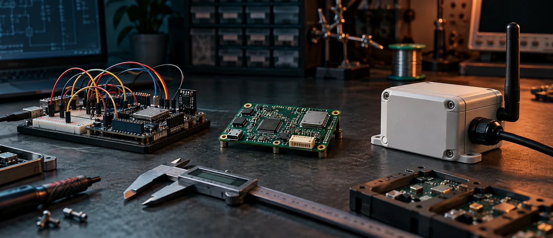
A development board is designed to make an idea easy to prove. It supplies a known power path, programming interface, reset circuit, clock, antenna arrangement, connectors, indicators, protection, and a layout already reviewed by the vendor. The prototype can therefore validate application behavior while borrowing infrastructure that the final product does not yet own.
A product starts when those borrowed assumptions become explicit engineering decisions. The custom board must operate from the real power source, inside the real enclosure, across expected temperature and radio conditions, with parts that can be purchased and assembled repeatedly. It must also be programmed, identified, tested, updated, and supported without relying on the engineer who built the first unit.
The transition is not complete when a smaller PCB boots. It is complete when the team has evidence that the design and the process produce known behavior.
Write the product contract before the schematic
Start with the conditions the hardware must serve. A prototype specification often says what the device does. A product contract also says where, for how long, under which limits, and how failure is handled.
Record at least:
- input supply range, source impedance, transients, reverse or misconnection risks, and expected power states;
- operating and storage environment, enclosure constraints, ingress assumptions, and service access;
- required radios, bands, antenna type, range conditions, coexistence, and target markets;
- sensors, actuators, connectors, isolation, protection, and external cable exposure;
- peak performance, duty cycle, sleep behavior, local storage, and acceptable data loss;
- manufacturing volume range, programming method, end-of-line test time, and traceability needs;
- supported lifetime, replaceable parts, update path, and ownership of field incidents.
These are not paperwork around the design. They determine regulator headroom, thermal paths, creepage and protection decisions, antenna placement, connector choice, test access, flash size, and whether a module or discrete SoC path is appropriate.
When a requirement remains unknown, mark it as an experiment with an owner and deadline. An explicit unknown can be tested. An implicit assumption becomes a late mechanical or electrical constraint.
Choose the integration boundary: module or SoC
A radio module can move several difficult responsibilities behind a vendor-controlled boundary: the SoC, crystal, flash, RF matching, and often a PCB antenna are integrated and documented together. That can reduce layout risk, simplify assembly, and provide a clearer starting point for radio authorization. It costs board area, constrains antenna placement and pin access, and may carry a higher unit price.
A discrete SoC can reduce size or unit cost and offer more layout freedom at sufficient volume, but the product team now owns more of the power distribution, clock, flash, RF trace, matching network, antenna tuning, assembly, and validation. Espressif's hardware guidelines are detailed because these physical relationships affect whether the chip performs as expected.
Make the choice from total engineering and lifecycle cost, not only BOM price. Include:
- expected volume and the value of board area;
- internal RF/layout experience and access to measurement equipment;
- schedule and cost of additional spins;
- assembly capability and package yield;
- antenna and enclosure constraints;
- supply continuity and approved alternatives;
- regulatory test scope in each market.
A certified module does not make the host product automatically compliant. Antenna selection, placement, enclosure materials, co-located radios, labeling, user instructions, and the exact host integration can change what testing or authorization remains. Confirm the plan with the module documentation and a qualified test laboratory before freezing the layout.
Rebuild the complete power and reset path
USB power on a bench is a generous environment. The product may see a battery with rising impedance, a long cable, an industrial rail, a charger transition, a load switch, a motor transient, or a solar source that rises slowly. Average current cannot describe whether the rail remains valid during radio transmit, flash write, sensor warm-up, or actuator start.
Espressif's ESP32 guidance explicitly calls out sudden current increases during transmission, local bulk and decoupling capacitance, stable rails before CHIP_PU, and power conditions where a monitor/reset supervisor can be more appropriate than relying on an RC delay alone. The exact circuit belongs to the chosen device, regulator, source, and PCB, but the evidence pattern is general.
Measure at the load, not only at the supply connector:
- startup and shutdown under minimum and maximum input;
- radio transmit and receive bursts;
- flash erase/write and simultaneous peripheral activity;
- transition between external power, charging, battery, and sleep;
- brownout, short interruption, slow rise, and repeated cycling;
- regulator temperature and efficiency across the real duty cycle.
Verify the state after recovery. A reset that returns immediately to the same peak load can become a loop. Persistent state should remain valid after power is removed at inconvenient points. A watchdog, brownout detector, and reset supervisor have different jobs; name which condition each one handles.
Own boot, programming, and recovery
Development boards make firmware loading and boot-mode selection almost invisible. A product needs an intentional path for manufacturing and service. Reserve access to power, ground, programming, reset, boot strapping, and any diagnostic interface required to distinguish assembly faults from firmware faults.
Strapping pins deserve a system review because external pull resistors, peripherals, test fixtures, and power sequencing can change their state during reset. Pin assignments also need to account for the exact package, flash/PSRAM configuration, boot behavior, and future board variants. Check the current datasheet rather than relying on a remembered pin map from the prototype.
Define at least three modes:
1. Manufacturing: program an authorized image, provision identity, run tests, and record results.
2. Normal operation: debug interfaces and boot controls expose no unintended authority.
3. Recovery/service: a documented process can diagnose or restore an eligible unit without returning every device to a shared insecure default.
Production test firmware and fixtures should be versioned artifacts. If a test changes, the manufacturing record needs to show which definition a unit passed.
Treat PCB layout as part of the circuit
At RF and fast digital edges, the schematic does not describe the whole design. Ground continuity, return paths, placement, via geometry, stack-up, decoupling loops, crystal routing, impedance, and coupling determine the circuit that was actually built.
Espressif's layout guidance recommends a continuous reference plane for the chip, RF, and crystal, controlled RF impedance, careful power distribution, short return paths, and specific antenna/module placement. Those are vendor requirements for a particular family, not decorative layout preferences. A two-layer board may be possible, but the resulting constraints and evidence burden differ from a four-layer design.
Review the PCB with fabrication data in hand:
- confirmed stack-up and impedance geometry from the PCB supplier;
- reference planes and return paths for every critical signal;
- placement and loop area of decoupling and protection;
- RF feed, matching options, antenna keep-out, and connector transition if used;
- crystal and flash/PSRAM routing against current vendor guidance;
- thermal spreading and enclosure contact assumptions;
- assembly clearances, fiducials, panelization, and test-point access.
Do not assume that a reference layout can be scaled, mirrored, or fitted around mechanical constraints without changing behavior. Preserve the relationships the vendor identifies, then verify the manufactured board.
Validate the antenna in the finished product
The antenna operates with the host PCB, enclosure, battery, cables, fasteners, display, user, and mounting surface around it. A module that performs well on its evaluation board can be detuned or shadowed after integration. Metal, ground, plastic composition, cable routing, and distance from the board edge all matter.
Plan antenna placement with mechanical design from the first PCB, not after the enclosure is fixed. Keep matching or measurement options recommended by the vendor, and test representative assembled units in the intended orientations and environments. For a discrete RF design, use qualified RF review and appropriate instruments. For a module, follow its antenna keep-out and approved antenna/integration conditions exactly.
Useful evidence includes conducted measurements where accessible, radiated pre-scan, receiver and connection behavior, coexistence with other radios or noisy electronics, and comparison across representative assemblies. RSSI from one desk test is not an antenna qualification.
Design the enclosure and PCB together
Mechanical design determines more than appearance. It sets connector strain, air volume, heat transfer, button and sensor behavior, antenna surroundings, assembly sequence, sealing interfaces, and serviceability. The PCB determines boss locations, cable bends, fastening loads, and where heat or light reaches the enclosure.
Maintain a shared model and a controlled interface document for board outline, keep-outs, component height, connector datum, mounting tolerance, antenna volume, thermal interfaces, and test access. Prototype representative materials and finishes before design validation. A transparent printed shell, open bench board, or hand-routed cable can hide interactions that appear in the production assembly.
Environmental claims need evidence at the assembled-product level. Component ratings do not automatically become product temperature, ingress, impact, UV, chemical, or lifetime ratings. Select tests from the actual use environment and applicable product requirements.
Build DFM and DFT into the design
Design for manufacturing asks whether the assembly process can build the board repeatedly. Design for test asks whether the process can distinguish a good unit from a specific failure quickly enough to control production. Both should influence the first custom board.
A useful manufacturing path can include:
- automated optical and electrical checks appropriate to the assembly;
- accessible programming and test pads with a fixture datum;
- current-limited first power and rail measurements;
- identity provisioning with duplicate prevention and an auditable result;
- checks for flash, memory, sensors, buses, indicators, buttons, and outputs;
- a bounded radio test that catches assembly and antenna-path defects;
- calibration where required, with calibration data tied to the unit;
- a final transition to the authorized production image and locked operating state.
Design the result schema with the fixture. Store board revision, serial or device identity, firmware and test versions, timestamp, station, calibration data, measurements, limits, and final disposition. A single PASS value cannot support yield analysis or field correlation.
Golden units and fixtures also need control. Their firmware, wiring, calibration, and allowed changes belong in the release system.
Version hardware and firmware as one compatibility system
The product will change. A regulator, sensor, flash device, antenna option, or pull resistor may be replaced. Firmware must know which differences affect initialization, limits, calibration, update eligibility, or diagnostics.
Give every board a readable revision and every programmed unit a durable identity. Define a compatibility matrix connecting hardware revision, assembly variant, bootloader, partition layout, firmware, configuration schema, and provisioning state. Avoid scattering board detection across unrelated drivers; establish one verified hardware description early in boot and expose it in diagnostics.
Component alternatives should be approved through evidence, not only matching distributor parameters. Compare electrical behavior, timing, layout footprint, software assumptions, environmental rating, lifecycle status, and test coverage. Some substitutions are equivalent; others create a new product variant that needs targeted validation.
The BOM release should identify manufacturer part numbers, allowed alternates, do-not-substitute items, stuffing options, and the evidence attached to each choice.
Use evidence gates from sample to process
Stage names vary between organizations, but an EVT/DVT/PVT model is useful when each gate answers a different question. Treat it as a working structure, not a certification.
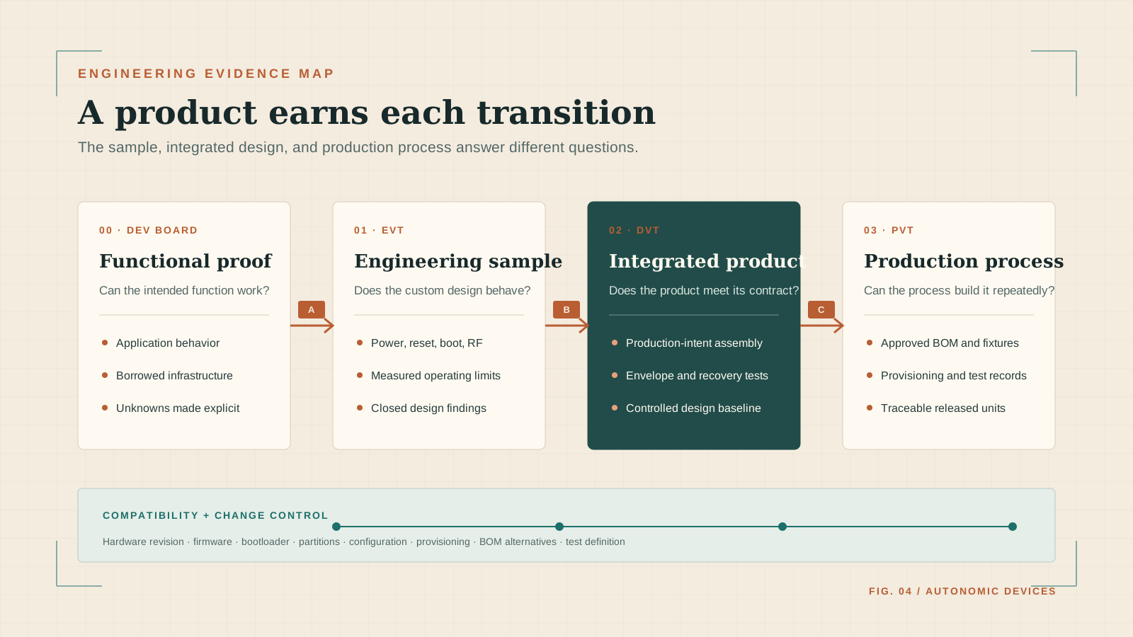
EVT: does the engineering design behave as intended?
Engineering validation units explore power, reset, clocks, interfaces, RF, sensors, thermals, programming, and failure behavior. They may contain measurement options and rework provisions. The output is not only a working sample; it is closed measurements, known limitations, and the next revision decision.
DVT: does the integrated product meet its requirements?
Design validation uses production-intent PCB, enclosure, components, firmware, and configuration. Test the operating envelope, mechanical interfaces, antenna performance, update/recovery, environmental behavior, pre-compliance, and representative misuse or fault conditions. Changes after this gate are controlled because they may invalidate evidence.
PVT: can the intended process build and verify it repeatedly?
Production validation exercises the contract manufacturer, approved BOM, assembly instructions, fixture, provisioning service, end-of-line tests, data capture, packaging, and release records. The question is not whether engineers can make the unit work. It is whether the defined process produces traceable units and identifies nonconformance.
For each gate, record entry criteria, sample and revision, test method, raw evidence, deviations, owner, and disposition. Passing with an unexplained anomaly is weaker than a known limitation with a boundary and corrective plan.
Plan compliance as a design input
Radio, EMC, electrical safety, environmental substance, labeling, privacy, and cybersecurity obligations depend on product type and markets. Identify the applicable path early enough that antenna, shielding, enclosure, connectors, power supply, documentation, and software support can still change.
Pre-compliance measurements are valuable before the final test campaign, but they are not approval. Likewise, modular radio approval can narrow work only when the integration stays inside its documented conditions. Maintain a compliance matrix with markets, standards or rules to confirm, responsible specialist, test configuration, samples, and evidence status.
NISTIR 8259 Rev. 1 provides a parallel reminder for connected products: manufacturers should address cybersecurity capabilities and customer needs before sale. Hardware identity, protected provisioning, update support, vulnerability intake, customer documentation, and end-of-support are part of the product system, not additions after PCB release.
Release the process, not only the Gerbers
A production release is a controlled set of compatible artifacts:
- schematic, PCB fabrication and assembly data, stack-up, and mechanical files;
- approved BOM and substitution rules;
- firmware, bootloader, partitions, configuration defaults, and signing state;
- programming, provisioning, calibration, and test definitions;
- fixture design and controlled golden references;
- assembly, inspection, rework, packaging, and handling instructions;
- verification reports, deviations, compliance evidence, and known limitations;
- version mapping, traceability schema, and support ownership.
Changes after release need impact analysis. A cheaper capacitor, different enclosure pigment, alternate flash, moved antenna, firmware timing change, or fixture update can affect evidence collected elsewhere. Change control is not bureaucracy around engineering; it is how the team knows which product it is supporting.
Product readiness checklist
Before a controlled pilot, require evidence that:
- the operating contract and unresolved assumptions are documented;
- the module or SoC boundary is justified by total lifecycle cost;
- power, reset, boot, programming, and recovery work under boundary conditions;
- PCB, RF, antenna, thermal, and enclosure behavior are measured on representative assemblies;
- manufacturing can program, identify, test, calibrate, and trace each unit;
- hardware and firmware compatibility is explicit;
- the BOM and alternatives are controlled;
- update, provisioning, diagnostics, and support responsibilities have owners;
- the validation and compliance plan matches the target product and markets;
- release artifacts can reproduce the tested unit without private engineering knowledge.
The development board remains valuable throughout this process as a reference, debug platform, and way to isolate software from custom-hardware behavior. It simply answers a narrower question. It proves that a function can work on known infrastructure.
A product earns its next gate when the team can explain the infrastructure it now owns, show the evidence behind its limits, and reproduce that evidence on units built by the intended process.
Sources and further reading
- Espressif: ESP32 Hardware Design Guidelines
- Espressif: ESP32 Schematic Checklist
- Espressif: ESP32 PCB Layout Design
- Espressif: ESP32 Series Datasheet
- Espressif Hardware Support
- FCC KDB 996369: Modules and Module Integration
- NISTIR 8259 Rev. 1: Foundational Cybersecurity Activities for IoT Product Manufacturers